Power Management IC
Very few resources seem to exist publicly documenting the PMIC and nearby components. This is a breakdown of the PMIC area of the Pi 5 board. It represents the aggregation of my own testing and information available on the Internet.
Replacement Sourcing
The primary power management chip on the PI 5 is a DA9091 which seems to have been purpose built for the Raspberry PI and as a result is not a general purpose component that you can source online.
That said, it does appear that PI Hut in the UK sells these.
Pad Reference
These were taken from a non working board, so needs verification. Measurements were taken on the board so you have to imagine the chip image was flipped 180 degrees on either of its vertical axis.
Ground was established without power and testing continuity.
5.3v was measured with the board plugged in and nothing else.This initial mapping was focused on what was connected directly to the USB C input. Its not an exhaustive list of 5v pads, but rather those pads which are getting 5v directly from the input rail. These in theory represent the input power to the PMIC itself.
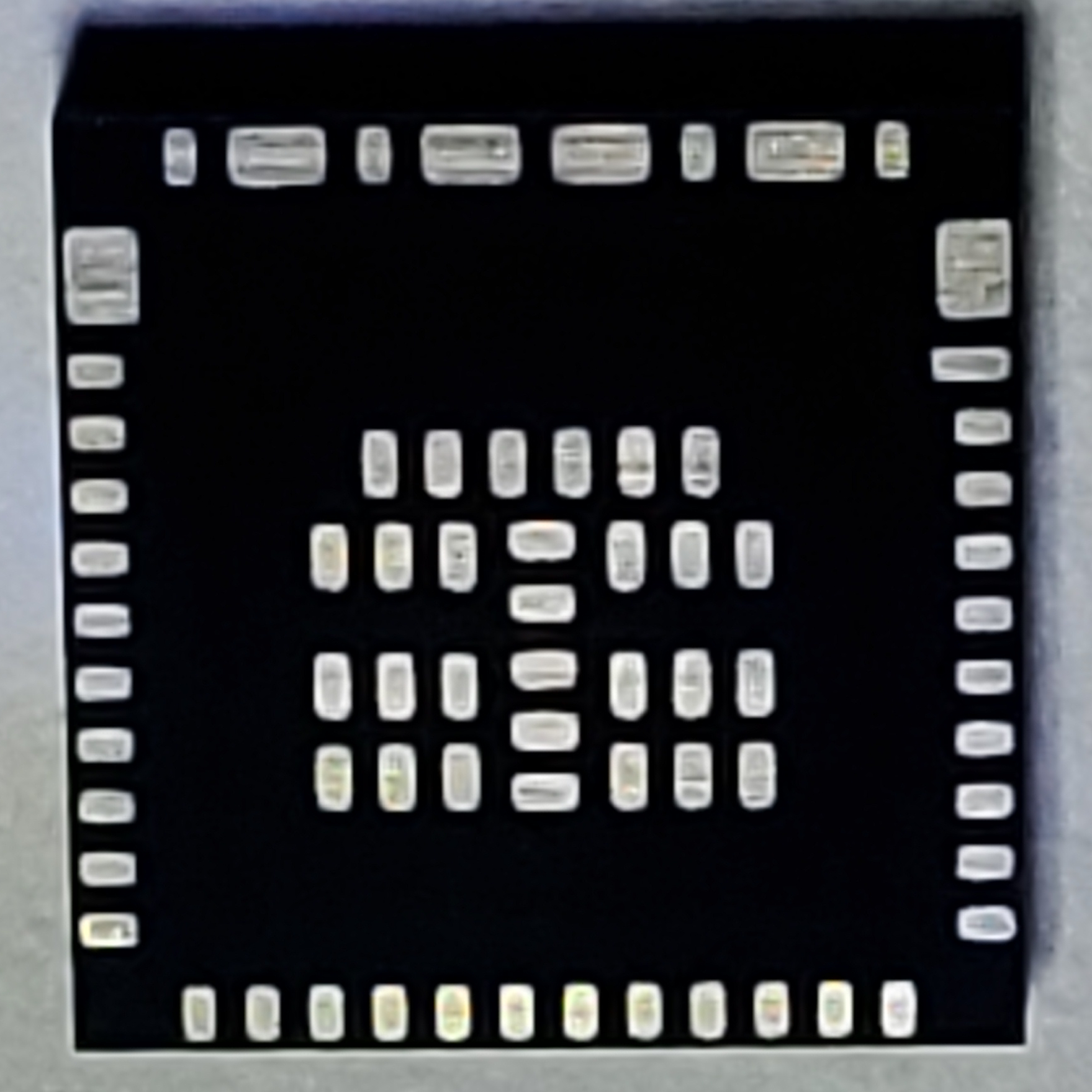
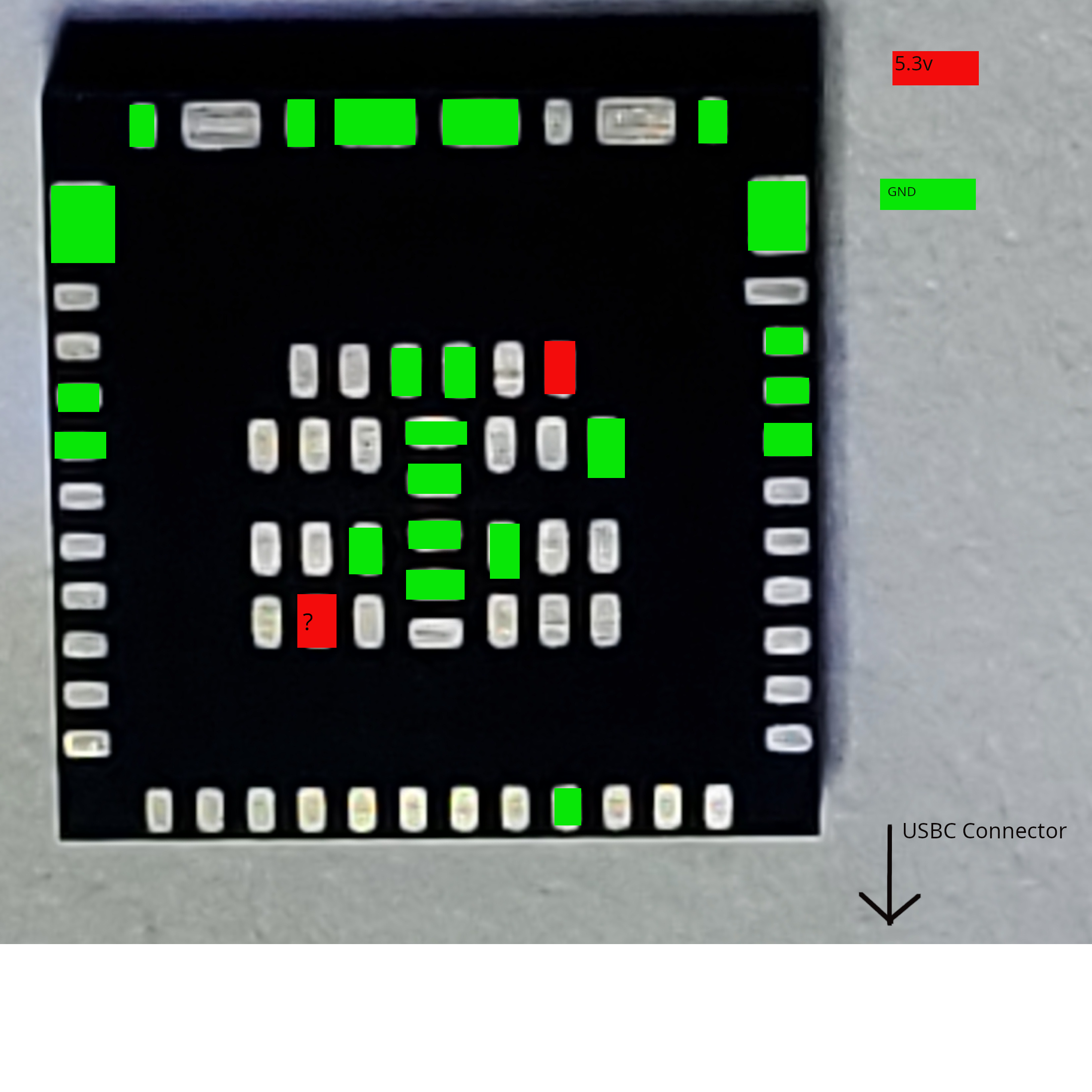
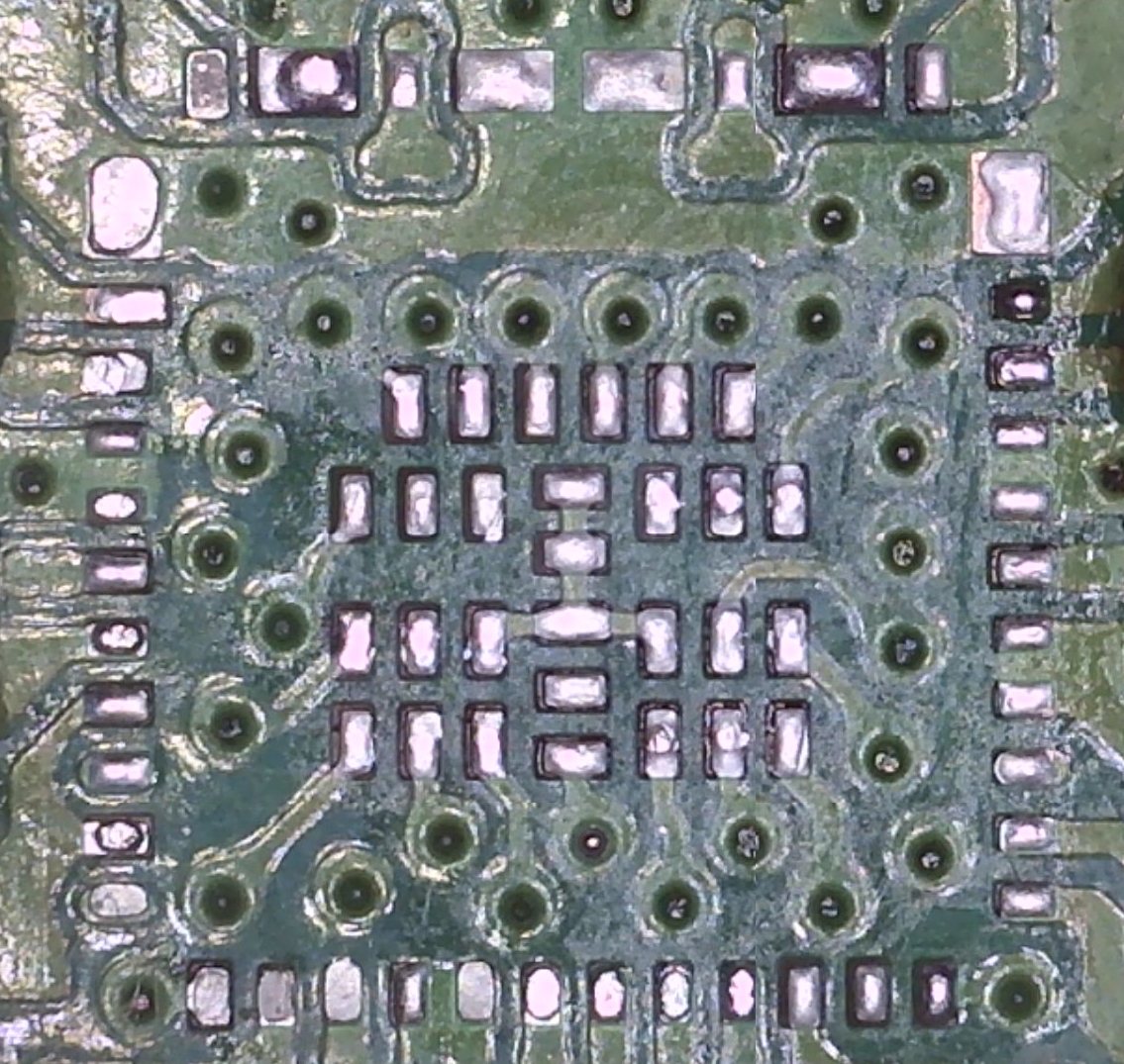
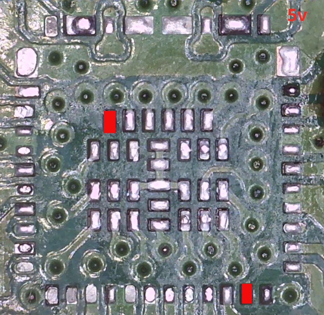
The following image was taken with the DA 9091 chip physically removed from the board showing the pad layout that is on the underside of the chip. Measurements were taken with the USB-C plugged in and the PMIC removed to try and highlight where 5v enters the PMIC
Area Breakout
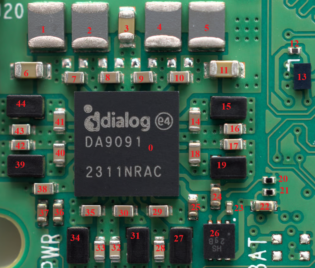
| # | Type | Package | Value | Power Rail | Links | Notes |
|---|---|---|---|---|---|---|
| 0 | QFN | multiple | This is the PMIC itself. As of 2026-05-29 Pi Hut seems to be the only place to source one.
Can be either Renesas or Dialog |
|||
| 1 | Inductor | Inductor Indentification | ||||
| 2 | Inductor | Inductor Indentification | ||||
| 3 | Capacitor | 0.8v | Voltage Source | |||
| 4 | Inductor | Inductor Indentification | ||||
| 5 | Inductor | Inductor Indentification | ||||
| 6 | ||||||
| 7 | Capacitor | 0402 | 5v | self-measured | ||
| 8 | Capacitor | 0402 | 22µF | 5v | Self measured | |
| 9 | Capacitor | 0402 | 5v | self-measured | ||
| 10 | Capacitor | 0402 | 5v | self-measured | ||
| 11 | ||||||
| 12 | ||||||
| 13 | ||||||
| 14 | Capacitor | 0402 | 5v | self-measured | ||
| 15 | Inductor | Inductor Indentification | ||||
| 16 | Capacitor | 0.8v | Voltage Source | |||
| 17 | Capacitor | 1.1v | Voltage Source | |||
| 18 | Capacitor | 0402 | 5v | self-measured | ||
| 19 | Inductor | Inductor Indentification | ||||
| 20 | ||||||
| 21 | ||||||
| 22 | ||||||
| 23 | Capacitor | 5v | self-measured | |||
| 24 | ||||||
| 25 | ||||||
| 26 | ||||||
| 27 | Inductor | Inductor Indentification | ||||
| 28 | Capacitor | 0.6v | Voltage Source | |||
| 29 | Capacitor | 0402 | 5v | self-measured | ||
| 30 | Capacitor | 0402 | 5v | self-measured | ||
| 31 | Inductor | Inductor Indentification | ||||
| 32 | Capacitor | 1.1v | Voltage Source | |||
| 33 | Capacitor | 1.8v | Voltage Source | |||
| 34 | Inductor | Inductor Indentification | ||||
| 35 | Capacitor | 0402 | 5v | self-measured | ||
| 36 | Capacitor | 0402 | 4.7µF | Value Source | 0402 4u7 6V3 X5R | |
| 37 | Capacitor | 0402 | 4.7µF | Value Source | 0402 4u7 6V3 X5R | |
| 38 | Capacitor | 0402 | 5v | self-measured | ||
| 39 | Inductor | Inductor Indentification | ||||
| 40 | Capacitor | 0402 | 5v | self-measured | ||
| 41 | Capacitor | 0402 | 5v | self-measured | ||
| 42 | Capacitor | 3.3v | Voltage Source | |||
| 43 | Capacitor | 3.7v | Voltage Source | |||
| 44 | Inductor | Inductor Indentification |
DA9091 Functional Reference
External Reference
The CM5 reverse engineering project by Tube Time provides detailed pin-level documentation of the DA9091 PMIC. The Compute Module 5 uses the identical DA9091 in the same QFN-71 (6×6mm, 0.4mm pitch) package, making this an invaluable cross-reference for Pi 5 repair work.
Applicability
The following pin assignments are derived from the CM5 reverse engineering project which uses the identical DA9091 PMIC. While pin functions are confirmed shared, the specific external circuitry (capacitor values, inductor values, PCB routing) may differ between CM5 and Pi 5.
Pin Function Summary (from CM5 reverse engineering)
| Parameter | Value |
|---|---|
| Package | QFN-71, 6×6mm, 0.4mm pitch |
| I2C Address | 0x38 |
| Pin(s) | Function | Description |
|---|---|---|
| 7, 9 | +5V | Main power input |
| 8 | VREG_INT | Internal regulator output |
| 10 | VREF | 3.3V reference output (VREF_3V3) |
| 11 | PWR_BUT | Power button input |
| 21 | HOTSWAP_DRAIN | Senses drain of DMG7430LFG |
| 22 | HOTSWAP_GATE | Drives gate of DMG7430LFG |
| 24 | VLOGIC | Logic supply |
| 43 | CC2 | USB-C CC2 line |
| 44 | CC1 | USB-C CC1 line |
| 47 | VBAT | RTC battery input |
| 50 | SCL | I2C clock |
| 51 | SDA | I2C data |
| 52, 53 | OSC | 32 KHz crystal oscillator |
| 56 | INT | Open-collector interrupt output |
| 62 | RUN | Power good / status output |
| 63 | EN_LOAD_SW | Enables secondary 3.3V and 1.8V rails |
| 65 | PMIC_EN | PMIC enable input |
Hot-swap function
The hot-swap function is built into the DA9091 — it directly controls the DMG7430LFG MOSFET gate (pin 22) while sensing the drain (pin 21), providing approximately 400 µs inrush current ramp-up time. This is not an external hot-swap controller; it is integrated into the PMIC silicon.
Power Rail Output Assignments
| Converter | LX Pin | Output Pin | Rail | Voltage | Notes |
|---|---|---|---|---|---|
| Buck 1 | 2 | OUT1 (49) | VDD_3V7_WIFI | 3.7 V | WiFi module supply |
| Buck 2 | 5 | OUT2 (55) | 3.3V main | 3.3 V | Primary 3.3 V rail |
| Buck 3 | 13 | OUT3 (61) | 1.8V main | 1.8 V | Primary 1.8 V rail |
| Buck 4 | 16 | OUT4 (71) | VDD_0V6 | 0.6 V | LPDDR4 VDDQ |
| Buck 5 | 19 | OUT5 (64) | VDD_1V1 | 1.1 V | LPDDR4 VDD2 |
| Buck 6 | 28 | OUT6 (60) | VDD_1V1_RP1 | 1.1 V | RP1 southbridge |
| Buck 7 | 31 | OUT7 (54) | VDD_0V8_BCM | 0.8 V | BCM2712 auxiliary |
| VCx (4-phase) | 34, 36, 39, 41 | VC_OUT (45) | VDD_BCM_CORE | ~0.8 V (variable) | BCM2712 core, DVFS-controlled |
| LDO | — | 25 | VDD_HDMI | — | HDMI supply |
| LDO | — | 23 | Unknown | — | — |
| VREF | — | 10 | VREF_3V3 | 3.3 V | Reference voltage |